How to write a parameterized universal shift register in verilog

A Shift registers is a very common design element in any digital design. This will be the only shift register you will ever need to write. The parameters in this code can be modified to create a shift register of any size and bit-width.
what is a shift register?
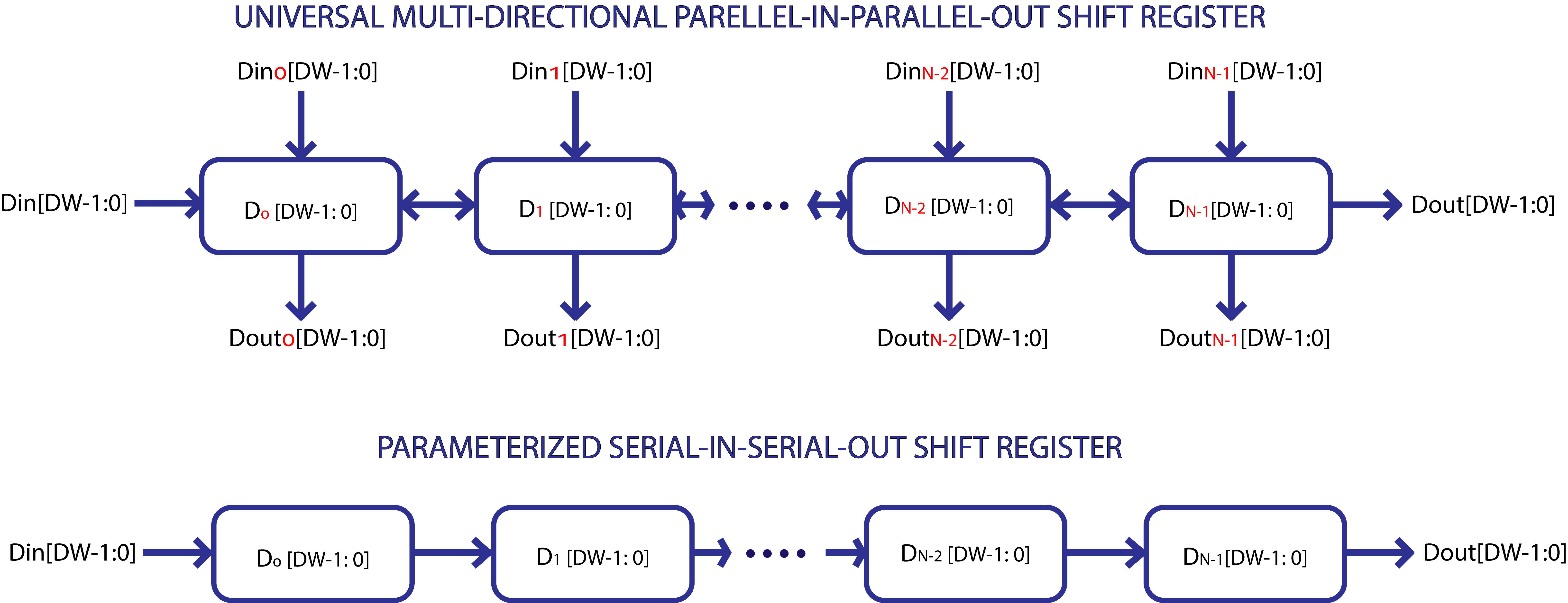
A shift register is a very basic design element very commonly used in digital designs generally for the purposes of delaying a certain data by a certain number of clock cycles. These are commonly called the SISO (Serial Input Serial Output) shift registers. There are also another kind called the SIPO (Serial Input Parallel Output) shift registers that are rarely used in applications like some exotic counter circuits. The ultimate version of the shift-register would be a PIPO(parallel-in-parallel-out) shift register which can be made to shift in either directions. The PIPO Shift Register is the most generalized form of a shift register and all the others mentioned above are just special cases of it. So let's code it!
A universal parallel-in-parallel-out shift register
 1
 2
 3
 4
 5
 6
 7
 8
 9
10
11
12
13
14
15
16
17
18
19
20
21
22
23
24
25
26
27
28
29
30
31
32
33
34
35
36
37
38
39
40
41
42
43
44
45
46
47
48
49
50
51
52
53
54
55
56
57
58
59
60
61
62
63
64
65
66
67
68
69
70
71
72
73
74
75
76
77
78
79
80
81
82
83
84
85
86
87
88
89
90
91
92
93
94
95
96
97 | `timescale 1ns / 1ps
module universal_shift_register #(parameter WIDTH = 8, parameter SIZE = 3) (
input clk, //clock
input ce, //clock enable
input rst, //reset
input load, //load
input dir, //dir=0 => right_shift dir=1> left_shift
input [WIDTH-1:0] data_in, //serial data input
input [WIDTH*SIZE-1:0] din, //parallel data input
output [WIDTH-1:0] data_out, //serial data output
output [WIDTH*SIZE-1:0] dout //parallel data output
);
reg [WIDTH-1:0] sr [SIZE-1:0];
reg load_delayed;
reg load_pulse;
//******************************************************************************
//Generating a load_pulse which lasts only one clock cycle long
//This prevents uncertainity as to what value is loaded owing to
//random duration of the incoming 'load' signal.
//eg. if 'load' is controlled by a user button we do not know exactly for
// how many cycles the button press is going to last. The value of 'din'
//could change in this period giving unexpected behaviour
// ┌──┐ ┌──┐ ┌──┐ ┌──┐ ┌──┐ ┌──┐ ┌──┐ ┌──┐ ┌──┐ ┌──┐ ┌──┐ ┌──┐
// clk : ┘ └──┘ └──┘ └──┘ └──┘ └──┘ └──┘ └──┘ └──┘ └──┘ └──┘ └──
// ┐ ┌─────────────────────────────┐
// load : └───────────────────────┘ └───────────
// ┐ ┌─────────────────────────────┐
// load_delayed: └─────────────────────────────┘ └─────
// ┐ ┌─────┐
// load_pulse : └───────────────────────┘ └───────────────────────────────────
always@(posedge clk or posedge rst)
begin
if(rst)
begin
load_delayed <= 0;
load_pulse <= 0;
end
else
begin
load_delayed <= load;
load_pulse <= load && ~load_delayed;
end
end
//*********************************************************************************
generate
genvar i;
for(i=0;i<SIZE;i=i+1)
begin:block
always@(posedge clk or posedge rst)
begin
if(rst)
begin
sr[i] <= 'd0;
end
else if(ce)
begin
if(load_pulse) //whenever we detect a load pulse, we load the register with new data
begin
sr[i] <= din[WIDTH*(i+1)-1:WIDTH*i];
end
else
begin
if(dir)
begin
if(i == SIZE-1)
begin
sr[i] <= data_in; //when there is no load pulse and ce = 1 we keep shifting the data
end
else
sr[i] <= sr[i+1];
end
else
begin
if(i == 'd0)
begin
sr[i] <= data_in;
end
else
begin
sr[i] <= sr[i-1];
end
end
end
end
else
begin
sr[i] <= 'd0;
end
end
assign dout[WIDTH*(i+1) - 1: WIDTH*i] = sr[i];
end
endgenerate
assign data_out = dir ? sr[0] : sr[SIZE-1];
endmodule
|
As already mentioned, the above Parallel-in-Parallel out shift register with multi-direction capabilities is rarely used in practice. It is used in some exotic circuits like Linear Feedback Shift Register (LFSR) based circuits and Pseudo-random-sequence-generators. However, a simpler version of this circuit, i.e. the Serial-Input-Serial-Output-shift register is very commonly used for purposes like introducing delays in the data-path and pipelining designs with too much combinational logic.
The Implementation
The below code implements a universal SISO shift register
 1
 2
 3
 4
 5
 6
 7
 8
 9
10
11
12
13
14
15
16
17
18
19
20
21
22
23
24
25
26
27
28
29
30
31
32
33
34
35
36
37
38
39
40
41 | `timescale 1ns / 1ps
module variable_shift_register #(parameter WIDTH = 8, parameter SIZE = 3) (
input clk, //clock
input ce, //clock enable
input rst, //reset
input [WIDTH-1:0] data_in, //data in
output [WIDTH-1:0] data_out //data out
);
reg [WIDTH-1:0] sr [SIZE-1:0]; //the register that holds the data
generate
genvar i;
for(i = 0;i < SIZE;i = i + 1)
begin
always@(posedge clk or posedge rst)
begin
if(rst)
begin
sr[i] <= 'd0;
end
else
begin
if(ce) //the shift register operates only when the clock-enable is active
begin
if(i == 'd0)
begin
sr[i] <= data_in;
end
else
begin
sr[i] <= sr[i-1];
end
end
end
end
end
endgenerate
assign data_out = sr[SIZE-1];
endmodule
|
Example usage scenarios
Rotation of bits in a register
 1
 2
 3
 4
 5
 6
 7
 8
 9
10
11
12
13
14
15
16
17
18
19
20
21
22
23
24
25 | universal_shift_register #(.WIDTH(3),.SIZE(1)) sr(
.clk(clk),
.ce(ce),
.rst(rst),
.load(load),
.dir(0),
.data_in(data_out),
.din(din),
.data_out(data_out), //data out is connected to data_in creating a loop, with the dir input we can control which
//direction we shift the data being fed to the register.
.dout(dout)
);
din[2] din[1] din[0]
+ + +
| | |
| | |
+----v-----+ +----v-----+ +-----v----+
| | | | | |
+-----> +--------> +---------> +----+
| | | | | | | |
| +----------+ +----------+ +----------+ |
| |
+--------------------------------------------------------------+
|
Variable delay module
 1
 2
 3
 4
 5
 6
 7
 8
 9
10
11
12
13
14 | variable_shift_register #(.WIDTH(3),.SIZE(4)) sr(
.clk(clk),
.ce(ce),
.rst(rst),
.data_in(input_data[3:0]),
.data_out(input_data_delayed[3:0]),
);
+----------+ +----------+ +----------+
| | | | | |
input_data +-----> +--------> +---------> +----> input_data_delayed_by_3_clocks
| | | | | |
+----------+ +----------+ +----------+
|
All the source Verilog files and their test benches can be found at the Github Repo
