Accelerating a 2-D image convolution operation on FPGA Hardware
This article demonstrates a functional system on a PYNQ-Z2 FPGA development board that accelerates a 2-D convolution operation by impelemnting it in programmable logic.
Part One - The Architecture Outline
Part Two - The Convolution Engine
Part Three - The Activation Function
Part Five - Adding fixed-point arithmetic to our design
Part Six - Putting it all together: The CNN Accelerator
Part Seven - System integration of the Convolution IP
Part Eight - Creating a multi-layer neural network in hardware.
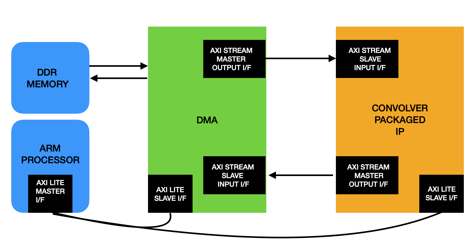
In the run up to building a fully functional neural network accelerator, it is important that we take a shot at full system integration of the IP we are writing. Before we add the entire complexity of a neural network with multiple layers, we should write the logic around our IP that would allow it to function as a part of a larger system through which the said acceleration can actually be materialised.
For this little experiment, let’s use the convolver IP that can take an image of any size and perform 2-D convolution over it.
The convolver IP, as it is in the current state needs the following things to become operational as a part of a larger system where a processor controls the data flow to an from the IP.
- AXI Stream slave interface the processor can use to feed the inputs to the convolver.
- AXI Stream master interface the convolver can use to send output to the processor.
- A bunch of configuration registers that can store the weights required for a particular convolution operation. For this we will be using an AXI Lite Slave interface that the processor can write to.
- Zooming out, a DMA block is required to pull data from the memory and manage the input and output AXI Stream interfaces to this IP.
The following block diagram shows the overall architecture and dataflow we want to achieve.
We will by using a PYNQ-Z2 board which is arguably the best suited platform for designing ML Hardware. Once we have a working system in place for the convolver IP, adding more elements to our IP and other bells and whistles to this setup should only be an incremental effort. This setup will also greatly help us in verifying our design over actual hardware as we continue to add features and eventually deploy a full neural network model.
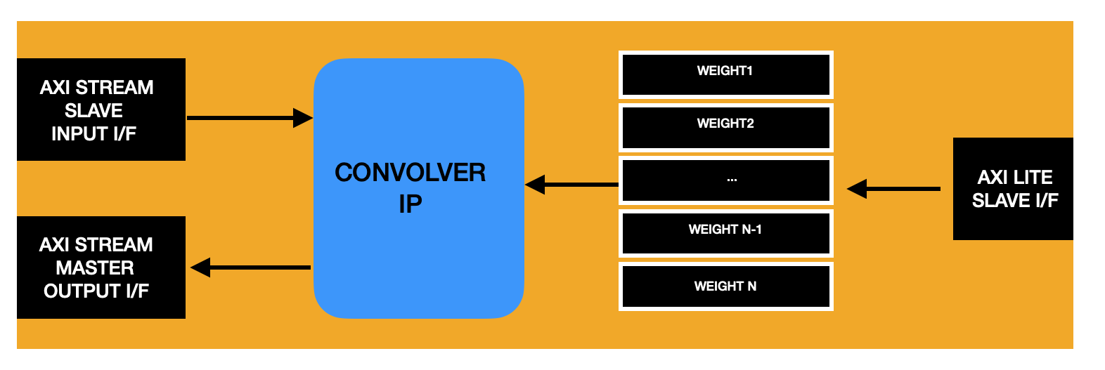
We begin by adding the AXI Lite slave interface to our wrapper. This will support a parameterized number of configuration register that the processor can access thorough its address space. I have stuck to the standard notation used by Xilinx for AXI interfaces in its IPs in order to make it easier for the IP packager later.
1 2 3 4 5 6 7 8 9 10 11 12 13 14 15 16 17 18 19 20 21 22 23 24 25 26 27 28 29 30 31 32 33 34 35 36 37 38 39 40 41 42 43 44 45 46 47 48 49 50 51 52 53 54 55 56 57 58 59 60 61 62 63 64 65 66 67 68 69 70 71 72 73 74 75 76 77 78 79 80 81 82 83 84 85 86 87 88 89 | |
That gives our IP a bunch of configurable address mapped registers.
Using these registers, let’s capture the weights in a format our IP requires.
1 2 3 4 5 6 7 8 9 10 | |
Now we need to take care of a specific nuance that comes with the AXI stream interface, or any streaming interface for that matter.
With that in place, let’s take care of the Streaming interfaces that will pump data in and out of the IP.
1 2 3 4 5 6 7 8 9 10 11 | |
Now Let’s see how to convert this interface into something our IP can work with:
The instantiation template to our IP looks like this:
1 2 3 4 5 6 7 8 9 10 11 12 13 14 15 16 17 18 19 | |
Some of these are straightforward, like the activation input can be directly connected to the incoming stream data signal s_axis_data and the conv_op output can be connected to the stream master data m_axis_data. The valid_conv signal also gets connected to the m_axis_valid pin.
Coming to the more tricky ones
- ce (clock enable) - This is simply the gating signal that allows the convolution logic to take a step forward. When this is low, the operation is frozen. Initially, its obvious that this should be connected to a combination of signals that indicates a valid AXI data beat on the input Slave interface, meaning:
1 | |
However, there is one thing that this logic is still missing, in a streaming interface of any kind, the master will be able to transfer data to the slave only when the slave is ready.
Output of the convolver is an AXI Master interface that feeds the slave that is the DMA. This transaction cannot happen if the processor de-asserts its ready signal.
Since there is no storage of any kind inside our IP, this means that the entire convolution pipeline should be halted whenever the DMA slave becomes unavailable.
which makes our clock enable signal:
1 | |
Since there is no reason to stall the pipeline for any other purpose other than the DMA slave not being ready, the ready signal of our convolution IP, which is slave to the DMA at the input streaming interface also becomes:
1 | |
There is one more signal left, that a lot of people who are beginners to the AXI interface forget. But this is very important because the DMA slave needs to be informed when a transaction from it’s master is complete. Otherwise it will stay waiting for more data beats and leave the channel stuck forever.
This is the m_axis_last signal, which will get connected to the end_conv output of the convolver IP.
Full System implementation:
The complete system block diagram looks something like this when being built for the. ZYNQ-7020 SOC that is on our PYNQ-Z2 board.
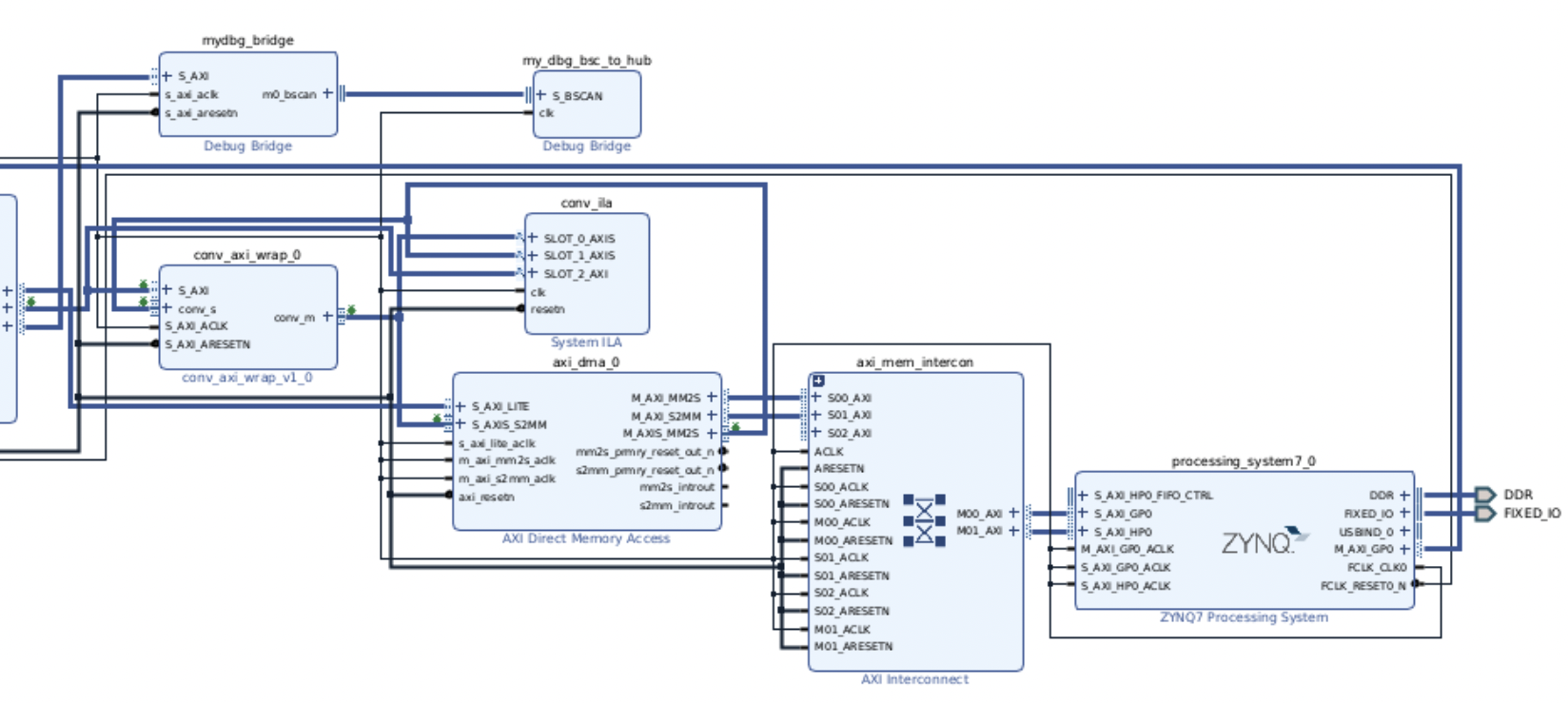
Here I’m using the chiprentals facilities to access a PYNQ-Z2 board along with a host linux system with all tools pre-installed.
There is extra debug logic on this system which is required for us to be able to look at the waveforms of actual hardware signals via the ILA. The debug bridge IP allows an XVC server to access these ILAs over a TCP connection through which the Vivado Hardware manager can let us see the actual signals in hardware like we would in a real oscilloscope. This is one of the coolest features enabled by the xilinx ecosystem and very soon I’ll write an article on it’s internal details.
Otherwise, the connections between the DMA to convolver IP and also the Processing System to the DMA are the same as what we had in our architecture diagram, only difference being the several AXI Interconnect blocks inserted by vivado to manage the addressing to different blocks.
Implementation Challenges
There was just one detail that ended up breaking the timing of our design during implementation at 100Mhz clock frequency. Once I dug into the path, it was obvious. The MAC (Multiply and Accumulate) operation code in our RTL currently looks like this:
1 2 3 4 5 6 7 8 9 10 11 12 13 14 | |
For the keen eyed, it should be obvious why timing failed on this path. This is a 32-bit multiplier followed by a 32-bit adder all clubbed into a single combo cloud. There is no reason why is should be this way and we can indeed cut down the critical path by a simple register re-timing optimization:
1 2 3 4 5 6 7 8 9 10 11 12 13 14 | |
This modification still preserves the single cycle count of this operation but significantly reduces the critical path by moving the adder logic after the flop-flop stage temp_q
Packaging the IP
Another super convenient feature of the xilinx ecosystem is that it let’s you package the IP in a reusable format and even does the versioning etc for it.
I will skip the details of this step but you should be able to find it pretty much anywhere else. It is a simple 1:1 mapping between the AXI protocol signals that vivado understands with the actual wrapper signals on your design.
Software platform
What we need to test this IP in a real world system is a processor that is closely coupled with FPGA fabric. In a typical FPGA only development board, it would be meaningless to compare the hardware performance with that of a CPU which is in no way connected to the FPGA.
The ZYNQ SOC on the other hand provides the perfect environment where two ARM cores are tightly coupled to FPGA fabric via a variety of AXI interfaces.
The PYNQ system let’s you use ipython notebooks through which you can effortlessly load the FPGA bitstream, instruct the DMA to fetch data from the DDR memory and pump it through the convolver IP and at the same time use pure software python functions to perform the same operation on the ARM processor.
Another luxury we have is that we can save ourselves from getting involved with extremely low level details of each IP and it’s corresponding driver.
Now, if you wish to fully understand an embedded linux system from top down then maybe getting into the drivers is a good idea. But if you are trying out ideas at the architectural level, you want a system that abstracts away these complexities for you so that you can focus on the bigger ideas.
Let’s start writing software for our newly integrated IP block:
1 2 3 4 5 6 7 8 9 10 11 12 13 14 15 16 17 18 19 20 21 22 23 24 25 26 27 28 29 30 31 32 33 34 35 36 37 38 39 40 41 42 43 44 45 46 47 48 49 50 51 52 53 54 55 56 57 58 59 60 61 62 63 64 65 66 67 68 | |
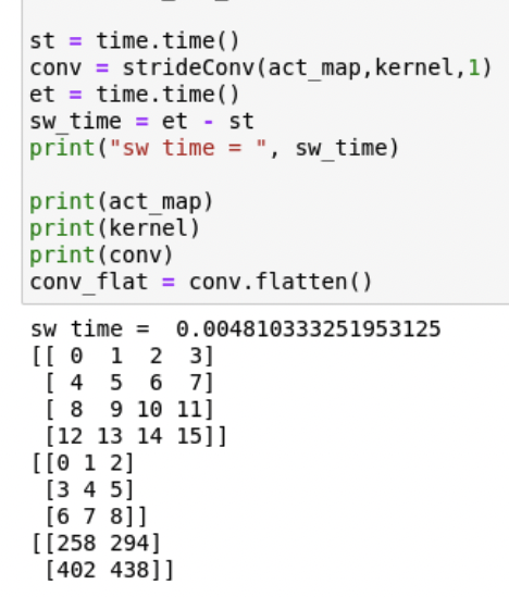
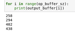
First let’s look at the output for a small matrix convolution just to see our system in action:
Software Execution:
Hardware Execution:
Not so surprisingly, the acceleration factor for this operation was 0.42 , meaning the hardware was slower than the software, which is obvious given the small size of the activation map. More time was spent in moving the data around than actual computation.
The speedup comes when we use larger matrices, things the size of an actual image.
I have summarized the experimental results in the following table:
| Image Dimentsion | Kernel Dimension | Speedup Factor |
|---|---|---|
| 4 | 3 | 0.42 |
| 600 | 3 | 134.15 |
| 1200 | 3 | 466.52 |
Note that the sw_time variable varies a lot from time to time even for the same activation matrix, this is because SW always has a non-deterministic latency, another reason to use FPGAs.
You can find all the code in this article at the github repository.